1. Definition and Suitable Applications
Metal etching in precision manufacturing usually refers to Photochemical Etching (PCE), also known as chemical etching or photo chemical machining (PCM). The process uses a photoresist mask to protect selected metal areas while an etchant chemically removes the unprotected areas, creating holes, slots, mesh patterns, profiles, half-etched bend lines, and identification marks.
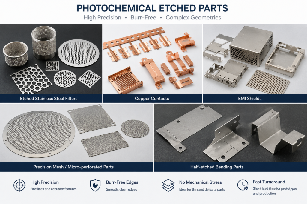
Photochemical etching is most suitable for thin metal parts with complex 2D geometries, dense hole patterns, fine slots, and frequent design revisions. Common materials include stainless steel, copper, brass, nickel alloys, and selected carbon steels.
| Suitable Part Features | Cases Better Suited to Other Processes |
|---|---|
| Fine holes, slots, mesh, and dense patterns | Thick structural or load-bearing parts |
| Thin spring parts, shields, filters, and screens | Deep high-aspect-ratio cavities |
| Half-etched bend lines, marks, and locating features | Extremely strict vertical sidewall requirements |
| Prototype and low-to-medium volume production | Very simple high-volume stamped parts |
2. Working Principle and Process Flow
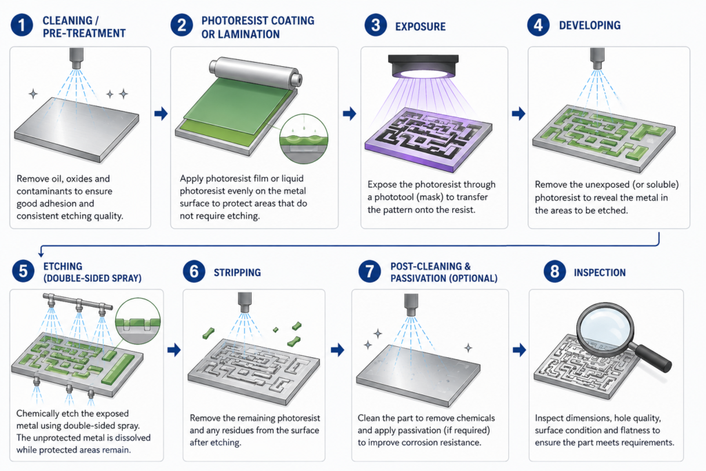
Photochemical etching removes metal through a controlled chemical reaction rather than mechanical cutting or laser melting. Areas protected by photoresist remain intact, while exposed areas are dissolved by the etching solution. This enables multiple holes, slots, profiles, and fine features to be processed on one sheet at the same time.
| Process Step | Main Function | Key Control Poin |
| Material cleaning | Removes oil, oxide, and particles | Surface cleanliness and consistency |
| Photoresist coating or lamination | Creates the chemical-resistant mask | Coating uniformity and adhesion |
| Exposure and development | Transfers CAD artwork to the sheet | Alignment and line-width compensation |
| Double-sided spray etching | Removes unprotected metal | Etch rate, temperature, solution concentration, spray pressure |
| Resist stripping and cleaning | Removes remaining mask and residues | Residual resist, stains, oxidation |
| Inspection and finishing | Confirms part quality | Dimensions, hole quality, appearance, flatness, protection |
A normal characteristic of chemical etching is undercut. The etchant removes material not only through the sheet thickness but also laterally beneath the mask edge. Therefore, hole diameter, slot width, bridge width, and outer profiles require design compensation.
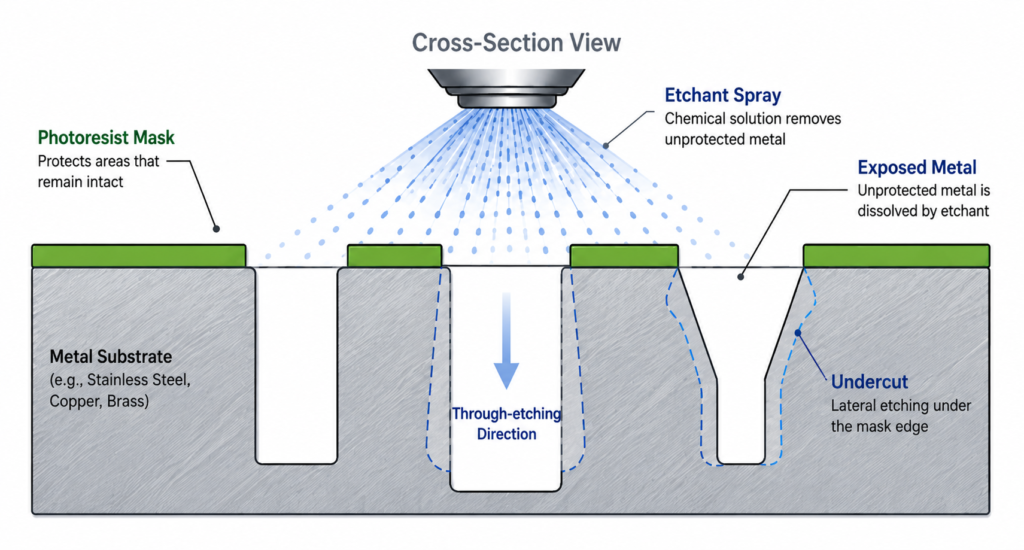
As a practical design guideline, the minimum through-etched hole diameter or slot width is commonly designed at approximately the material thickness or larger. Actual capability depends on material type, sheet thickness, feature density, geometry, and the supplier’s validated process window.
3. Common Applications, Design Capability, and Advantages
Common Applications
| Industry | Typical Etched Parts |
| Consumer electronics and telecom | EMI/RF shields, contact springs, lead-frame components, encoder discs, metal meshes |
| Medical devices | Surgical blades, micro filters, sensor parts, precision screens |
| Automotive and new energy | Sensor springs, precision filters, connector parts, fuel-cell bipolar plate features |
| Industrial equipment | Valve plates, flow-control parts, filters, metal nameplates, encoder components |
| Aerospace and instrumentation | Precision grids, thin spring elements, apertures, mesh panels, shielding parts |
Dimensional capability is closely related to material thickness. For thin-gauge sheet metal, commonly achievable etching tolerances may reach approximately ±0.025 mm under controlled conditions. As thickness increases, tolerances are often evaluated around ±10% of material thickness, depending on feature geometry and supplier capability.
| Comparison Item | Photochemical Etching Characteristic | Engineering Value |
| Tooling | Digital artwork rather than hard stamping dies | Faster prototype changes and lower tooling risk |
| Processing method | Multiple features etched simultaneously | Efficient for dense holes, slots, and complex flat profiles |
| Heat effect | No laser melting edge | Avoids local heat-affected zones |
| Mechanical stress | No stamping force during profiling | Suitable for thin and easily distorted parts |
| Edge condition | Normally free from conventional punching burrs | May reduce secondary deburring requirements |
| Limitation | Undercut exists; thick material capability is limited | Not a replacement for every stamping, laser, or CNC application |
The main value of photochemical etching is not replacing all machining processes. It is most effective for complex, thin, multi-feature metal parts that require fast design changes and low mechanical or thermal influence.
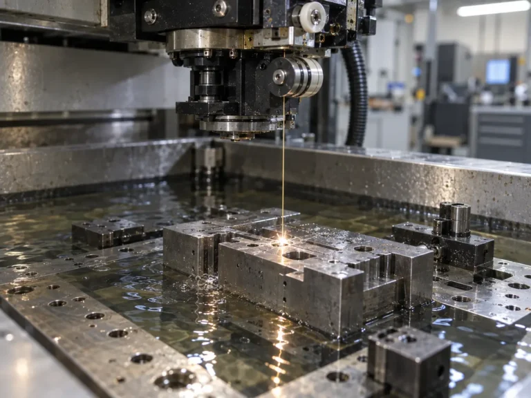
For thick, simple, high-volume parts with strong structural requirements, stamping, laser cutting, CNC machining, or wire EDM may be more economical or technically appropriate.
FAQ
1. What is chemical etching and how does it work?
Chemical etching (also known as photochemical machining) is a subtractive manufacturing process that uses light-sensitive photoresists and chemical etchants (like ferric chloride) to precisely dissolve unwanted metal areas. It creates intricate, burr-free, and stress-free precision metal parts from thin sheets without altering the material’s properties.
2. What are the advantages of chemical etching vs. stamping or laser cutting?
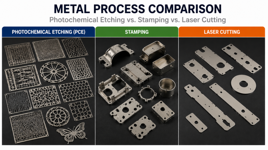
Compared to traditional metal stamping or laser cutting, chemical etching offers zero thermal distortion, burr-free edges, and requires no expensive hard tooling. Digital phototools can be created in hours, making it highly cost-effective and flexible for both rapid prototyping and high-volume precision production.
3. Which metals can be chemically etched?
Chemical etching is compatible with a wide range of metals, including stainless steel (all grades), copper and its alloys (brass, bronze, beryllium copper), aluminum, nickel alloys, and titanium. It can process materials with thicknesses ranging from 0.010 mm up to 2.5 mm.
4. What tolerances can be achieved with photochemical etching?
Typically, chemical etching can achieve an exceptional tolerance of ±10% of the material thickness (down to ±0.025 mm or ±0.001 in). The exact tolerance depends on the material type, grade, and specific geometry of your design.
5. What are the common industrial applications of etched metal parts?
Etched components are widely used in demanding industries like electronics (EMI/RFI shielding, lead frames), automotive (shims, gaskets), aerospace (fuel filters, sensors), and medical devices (stents, surgical blades), where high precision and edge-perfection are critical.
6. How much does chemical etching tooling cost, and what is the lead time?
Unlike hard dies that cost thousands of dollars, chemical etching uses digital phototools which typically cost under $150 to $200 and can be modified instantly. Prototyping lead times are usually 3 to 5 days, while production orders can be fulfilled in 1 to 2 weeks.